Research
Current Research Topics
1. very high efficiency novel solar cells
The world’s annual energy consumption stands at approximately
5x10²⁰ Joules and is predicted to rise to over 7x10²⁰Joules by the year
2035. Currently demand is mainly met using fossil fuels (81.2%) while
renewable sources account for 12.8 % and nuclear fission 5.8%. With only finite
fossil fuel reserves and persistent concerns over nuclear safety, it is a
priority to meet as much of the increasing demand as possible with renewable
sources.
Of renewable sources sun is by far the most abundant source of energy (more
energy from the sun reaching the earth’s atmosphere every 46 minutes than
mankind uses in a year). This energy can be converted directly from light to
electricity by photovoltaic cells. To date the highest efficiency solar cells
have been GaAs based tandem cells, achieving efficiencies of 32% for AM1.5G for
un-concentrated radiation and 42.3% for AM1.5D at 406 times concentration. The
band gap of a solar cell directly affects the maximum efficiency due to low and
high wavelength cut-offs. In 1992 it was discovered that the addition of a small
amount of nitrogen to GaAs leads to a large red shift in the materials band gap
as well as a decrease in its lattice constant5. This combined with the addition
of indium which also decreases the band gap but increases the lattice constant
allows the quaternary alloy Ga1-xInxNyAs1-y to have band gaps significantly
lower than GaAs but remain lattice matched to it. However, the addition of
nitrogen also causes a reduction in the minority carrier mobilities and
lifetimes leading to low diffusion lengths making it impossible to produce
efficient GaInNAs solar cells using conventional designs. In order to overcome
this problem, at Essex we aim to design and study GaInNAs solar cells using two
novel approaches. The first is the multiple quantum well (MQW) solar cell design
where GaInNAs quantum wells are combined with GaAs solar cells extending the
spectral response towards infrared with the aim of improving the current
matching in tandem solar cells. The second approach is to use an n-i-p-i doping
design which overcomes the problem of low diffusion lengths by consisting of a
number of thin n and p type layers connected by selective contacts.
2. Gunn Laser
It is well known that Near Infrared Radiation (NIR) is emitted
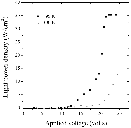
from propagating high-field domains in a GaAs Gunn device. We have reported the
spontaneous emission characteristics from such devices as a function of
temperature and electric field. We have also predicted that spontaneous emission
may evolve into stimulated-emission in a Gunn device when it is placed in a
Fabry-Perot cavity. Indeed the operation of a Fabry-Perot Gunn laser has been
demonstrated by us recently at T ≥ 95 K.
The results are analyzed in detail and compared with model
calculations.
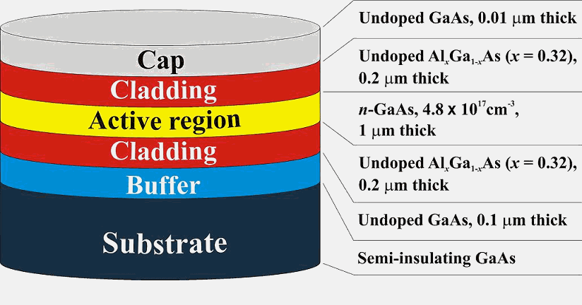
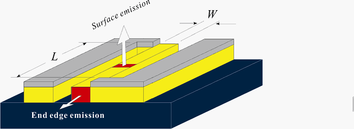
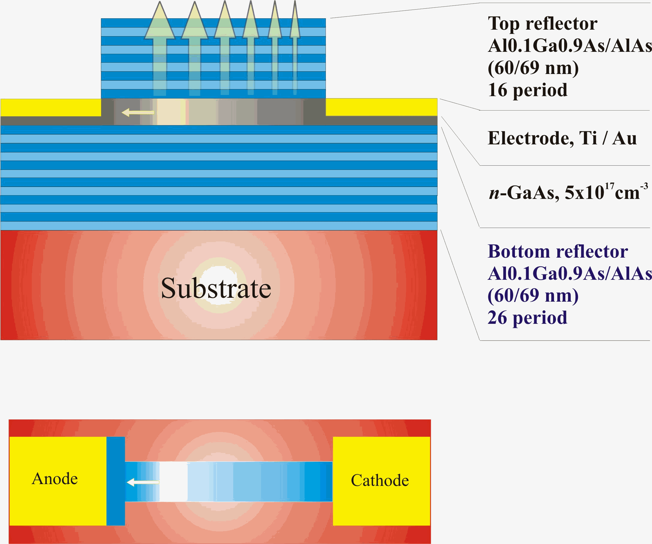
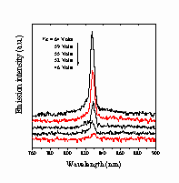
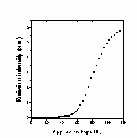
The aim of the current work is to study Gunn Vertical Cavity
Surface Emitting Laser (VCSEL) which is a truly monopolar device. The principle
of the operation is based on the band to band recombination of impact ionized
non-equilibrium electron-hole pairs in the propagating high field domains along
the Gunn diode, which is biased above the negative differential resistance
threshold, and placed in a vertical micro cavity. In conventional Vertical
Cavity Surface Emitting Laser (VCSEL) structures, unless specific measures such
as the addition of oxide apertures and use of small windows are employed, the
lack of uniformity in the density of current injected into the active region can
reduce the efficiency and delay the lasing threshold. In a vertical-cavity
structured Gunn device, however, the current is uniformly injected into the
active region independently of the distributed Bragg reflector (DBR) layers.
Therefore, lasing should occur from the entire surface of the device.
Furthermore, because the light emission from Gunn domains is an electric field
induced effect, the operation of VCSEL are independent of the polarity of the
applied voltage defining a surface emitting optical exclusive OR logic gate. Red
-NIR VCSELs emitting in the range of 630-850 nm are plausible when Ga1-xAlxAs
(x < 0.45) is used the active layer, making them candidates for light
sources in plastic fibres (POF) based short-distance data communications.
3. Optoelectronics based on InN and In-Rich
GaInN
The In1-xGaxN material has the widest
range of direct gap of any compound semiconductors extending from 0.7 eV to 3.2
eV which can be utilized in optoelectronic device applications over a wavelength
range, from infrared to ultraviolet as shown in the including very many key
wavelengths for applications in the medical, environmental and communications
fields.
A recent press release by Lawrence Berkeley National Laboratory
says of In1-xGaxN: "....It is as if nature designed this
material on purpose to match the solar spectrum..... The cost (of solar cells)
will be the same order of magnitude as traffic lights.... (They will be) so
efficient and so cheap that it could revolutionize the use of solar power
The growth of high quality InN and Indium rich In1-xGaxN
have been achieved only recently but an intense research effort has been aimed
at understanding the details of the electronic and optical properties of the
these alloys.From optoelectronic devices point of
view the first commercial target is likely to be multilayer solar cells. In the
ternary, In1-xGaxN, a Ga concentration of
 should produce direct
bandgaps between 0.7 and 1.9 eV to match perfectly the useful part of the solar
spectrum. Very high efficiencies could be achieved by the use of multilayers
with improved radiation hardness over conventional cells. The growth of high
quality epilayers of InN (x=0), with intrinsic electron densities of n> 2 10
17 cm-3), mobilities in excess of 2000 cm2 V-1
s-1 implies that InN itself, has immediate potential applications in
high power high frequency FETs and terahertz devices for sub-millimeter wave
imaging.
Potential applications of the In1-xGaxN
Technology
Material
GaN
InN
| (360) | |
| | |
|
| | (1610)
Wavelength (nm)
300 600
900 1200
1500
Technological Applications
Displays/lighting 370,470,540 640 (violet,
blue, green, red)
Storage 405
650 780 (BD, DVD, CD)
Solar cells
-----multilayers
profiled in wavelength to solar spectrum with high
efficiency-
Communications 510 (POF) 650
(free-space line-of-sight)
1300(silica) 1550
(silica)
Pumps 810
980, 1000, 1050 14xx,
1480)
(YAG,
EDFA, TDFA, PDFA)
(Raman, EDFA)
Sensing
760
1540
(Oxygen)-----Many spectroscopic lines------ (ammonia,
Methanol)
PDT (to match photo-sensitizers for specific
treatment)...
Surgery
488,532
1064 1320, 1440
(Argon, YAG
replacement) (YAG replacement)
High speed high power FETs High
carrier density (1014 cm-2) and low
effective mass
Terahertz devices
Due to transient photo-carrier currents, stronger magnitude
than any other
semiconductors
|
Acronyms:
BD - Blu-ray disc, CD - compact disc, DVD - digital versatile disc, EDFA -
erbium-doped fibre amplifier, PDFA - praseodymium-doped fibre amplifier,
PDT - photo-dynamic therapy, POF - plastic optical fibre, TDFA
- thulium-doped
fibre amplifier, YAG - Yttrium Aluminum Garnet
4. Optoelectronic devices based on dilute nitrides
III-V Semiconductors are indispensable for today's
optoelectronic devices such as semiconductor lasers used in optical
communication systems. Likewise, this class of materials is dominant in key high
frequency electronics components for wireless communication systems. The
miscibility of binary III-Vs and the possibility to stack such layers of various
compositions and doping levels is crucial for all these applications. The
tailoring of hetero-structure properties is limited by the different lattice
constants of the binary III-Vs, which limit the range of useful compositions and
thereby the range of available band gaps. Thus, on the two most commonly used
substrate materials, GaAs and InP, the band edges can be tailored to allow only
a limited range of useful wavelengths of a maximum of 1200nm for GaAs-based and
about 2100nm for InP-based materials. Moreover, the alignment of the band edges,
which is highly important for the performance of devices, cannot be tailored by
the combination of conventional materials at all. These limitations
encountered in InP and GaAs based devices can be greatly reduced by
incorporating a few percent of nitrogen as a group V element into GaAs or
InGaAs,
i.e. by creating the so-called "dilute nitrides". In dilute nitrides, unlike in
all other cases, where a reduction in band-gap energy is achieved by inserting
an element that increases the lattice constant, N effectuates this and at the
same time reduces the lattice constant. Thus smaller band-gaps can be achieved
and the unusual role of N in the lattice also allows a tailoring of band
alignments. Both of these effects have opened up a new dimension of band-gap
engineering.
The low loss window of optical fibre has recently been
extended to cover 1.3 to 1.7 m m, significantly
increasing the potential capacity of optical networks. As a result,
optoelectronic devices (such as lasers, detectors, filters and optical
amplifiers) operating in this wavelength range dominate photonics research. Many
of these devices are enhanced using distributed Bragg reflectors (DBR's) to
control the optical field. Typical examples include vertical cavity surface
emitting lasers (VCSELs), resonant cavity enhanced (RCE) photodetectors,
RCE-LEDs and vertical cavity semiconductor optical amplifiers (VCSOA).
Unfortunately, the device requirements are not met by
conventional GaAs or InP based materials, such as InGaAs/GaAs or InGaAsP/InP.
Most GaAs-based material systems only allow device operation out
to ~1.2 μm, while InP-based systems suffer from poor thermal stability
(lowering
efficiency) and low refractive index contrast (hindering DBR fabrication). This
low index contrast means that many layers are required to achieve high
reflectivity InP-based DBRs. Growing thick uniform stacks without defects
is very difficult and introduces the additional problem of high series
resistance, which retards device dynamics. These problems can be avoided by
fusing AlGaAs/AlAs DBRs to the active layers, however, this complicates
fabrication, increasing cost and may result in un-reliable devices.
Dilute nitrides avoid many of the problems associated with
conventional arsenides and phosphides. Incorporating a few percent of nitrogen
into (In)GaAs has a profound influence on its electronic properties. In most
III-V materials, substituting an element for one with a smaller atomic radius
reduces the lattice constant and increases the bandgap. However, Weyers et.al
found that replacing a fraction of arsenic atoms in GaAs with smaller N atoms,
rapidly reduces the bandgap. In addition to giving access to smaller bandgaps,
nitrogen allows band alignment, lattice constant and strain to be tailored,
opening up a new dimension of band engineering.
The quaternary alloy GaInNAs is attractive for a range of
devices, offering advantages over conventional narrow gap materials. GaInNAs
quantum wells (QWs) can be grown pseudomorphically on GaAs, giving strong
carrier confinement (hence thermal stability) and compatibility with GaAs
technology, including AlGaAs/AlAs DBRs. GaNAs is less relevant to devices,
however, it does allows investigation into the physical properties of dilute
nitrides.
(a)
(b)
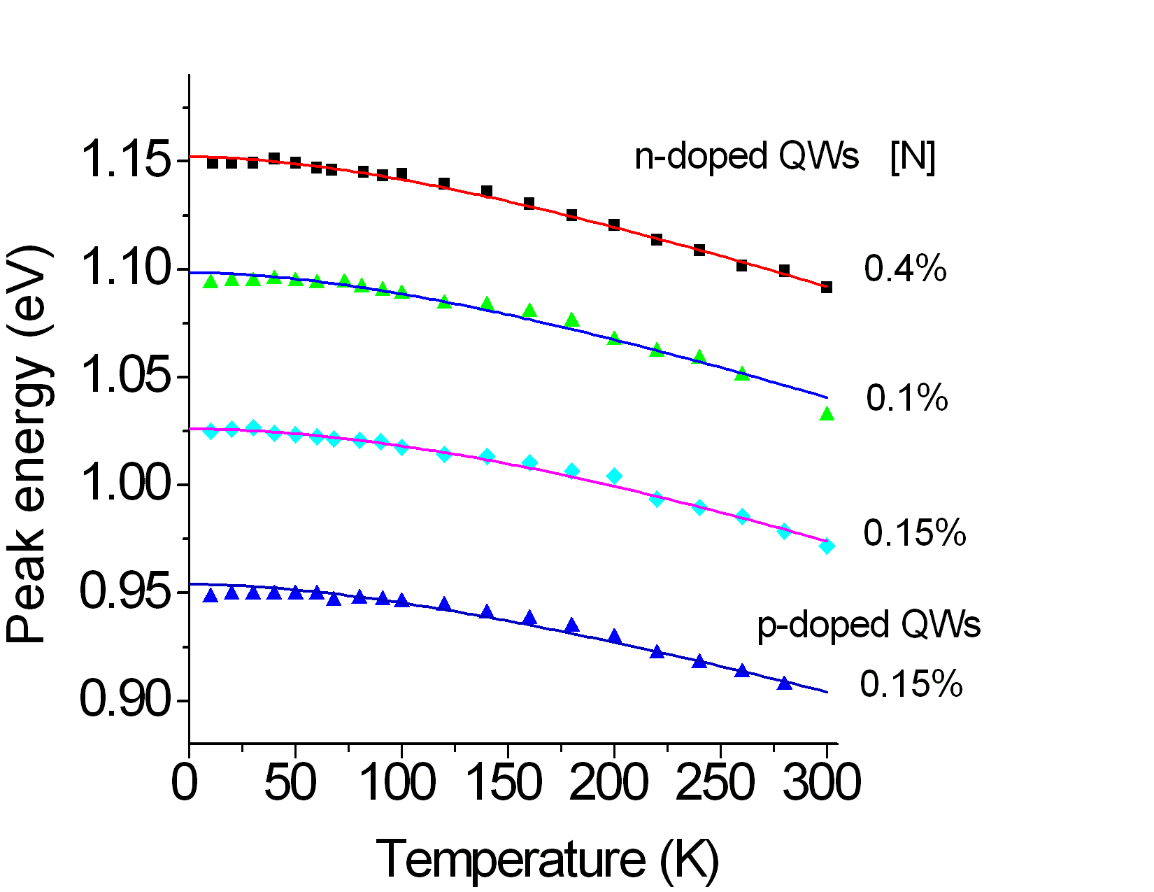
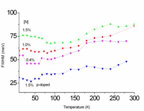
Temperature dependence of the PL peak energy (a,) and the FWHM
(b) of the modulation doped samples for different nitrogen compositions.
A wide range of novel devices could benefit from dilute
nitrides. Devices already demonstrated include VCSEL's, VCSOAs,
RCE-photodetectors, RCE-LEDs, multijuction solar cells, modulators and
heterojuction bipolar transistors (HBTs).
Commercially, the most important devices are for inexpensive optical fiber data
transmission at 1300 nm for metro-area links over 10 to 20 km These links are
presently considered to be the bottleneck for large-scale optical communications
and constitutes a very large market volume. Rapid progress has already led to
the demonstration of high quality 1300 nm dilute nitride laser diodes on GaAs
and even 1300 nm VCSELs. Emission from dilute nitride devices has even been
pushed above 1500 nm, potentially useful for long haul links.
One major difficulty with dilute nitride growth is
maintaining good optical quality as nitrogen is incorporated. This has provoked
extensive work to establish the factors effecting optical quality, such as
composition, growth and annealing conditions. Techniques, such as PL, surface
photovoltage spectroscopy (SPS), deep level transient spectroscopy, spectral
photoconductivity and STEM, etcare commonly used to investigate the
presence of structural and compositional fluctuations, impurities and defects.
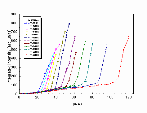
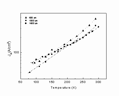
L-I measurements for the 1600 um SQW
laser
Threshold Carrier Density versus temperature
In order to analyse and improve the design of functional
devices based on dilute nitrides, and further predict the ultra-fast novel
devices based on these materials, a through understanding of electron transport,
particularly at high electric fields, is necessary. Hot-electron dynamics for
longitudinal transport in degenerate 2D GaAs and III-N structures are well
documented, where the production of non-equilibrium LO phonons (hot phonons) are
well-known to slow down the hot electron energy relaxation.It is
also shown that at high electric fields, the randomization of the hot phonon
distribution may take place via the elastic scattering of phonons with, for
instance interface roughness and alloy fluctuations, hence the drift of hot
phonons can be neglected. If the momentum relaxation of phonons is faster than
their decay time, the change in the electron momentum between the emission and
re-absorption of hot phonons can be quite large. Hence the production of hot
phonons, with a finite lifetime may also enhance the momentum relaxation rate.
The electron drift velocity at high fields is therefore reduced and
consequently, inter-valley and real-space transfer negative differential
resistance may be quenched.
In dilute nitrides the almost inevitable presence of nitrogen
clusters, impurities, interface imperfections and dislocations will provide
ample sources for phonon momentum scattering. The population of non-equilibrium
phonons is therefore expected to be strongly non-drifting, particularly in the
region where hot phonon effects are important. Therefore, the reduction in the
high-fields drift velocity saturation is expected and the negative differential
resistance may be inhibited.The aim of the work at Essex is to
explore whether the observed electron drift velocity at high fields can be
explained by invoking a mechanism involving the production of non-drifting hot
phonons.
The large bandgaps of GaNand AlN make these materials
promising as the ingredients of high-power electronic devices. The general aim
is to make devices that can produce microwave power of the order of 100 W at
X-band (8-12 GHz). High power entails a high electron concentrations and
densities over 1.0 1013 cm-2 which, in AlGaN/GaN
heterostructures are routinely observed in Hall measurements. Such densities are
achieved as a direct consequence of the large spontaneous and strain-induced
polarization in the AlGaN barrier. Thus, there is no need to add donors, unlike
the case in GaAs-based structures. This independence on impurity concentration
is a consequence of the symmetry property of wurtzite, which allows spontaneous
polarization to occur, and its piezoelectricity and of the strong polarity of
GaN and its alloys with Al. Electron transport under these conditions has the
novel possibility of taking place in the absence of impurity scattering while at
the same time involving a high density of electrons, which is a unique situation
in semiconductor physics. It has been shown recently that when impurity
scattering can be neglected and when scattering is dominated by acoustic
phonons, then instabilities, electron cooling and squeezed electron states may
be observed.
At the present time device performance is hampered by the low
crystalline quality of MBE and MOCVD material, consequent on the lack of
lattice-matched substrates. In spite of the effect of dislocations at densities
exceeding 109 cm-2 and the effect of background impurity densities of order of
1018 cm-3, room-temperature Hall mobilities of electrons
in the quasi-2D channel of an FET are frequently within 25% of the
phonon-limited value of about 2000 cm2/Vs. In contrast, mobilities in bulk GaN
are much lower.
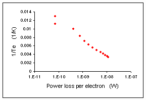
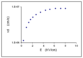
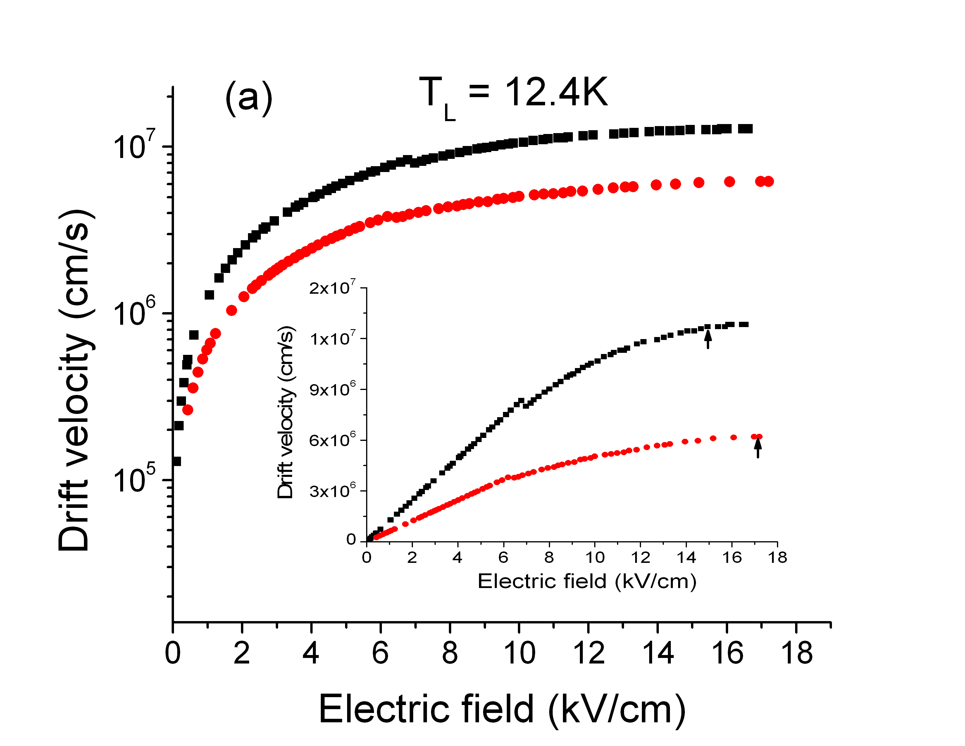
(a)
(b)
Figure 1. (a) Power Loss per electron versus electron
temperature. (b) Electron drift velocity versus applied electric field at T=77K
Hot-electron transport in AlGaN/GaN heterostructures provides invaluable
information on scattering mechanisms at high fields relevant to FET devices. The
conduction-band structure of GaN, like GaAs, is suitable for the
electron-transfer effect and associated negative differential resistance (NDR)
at high electric fields, and there are several reports describing the
velocity-field curve in bulk material predicted by Monte Carlo simulation
Another aspect of the large bandgap of GaN is the capability
of that material to withstand very high fields (>1 MV/cm) before breaking down.
Ridley and co workers recently calculated the conduction-band structure of GaN
in its wurtzite and in its zinc blende forms using updated experimental input to
the empirical pseudopotential model. On this basis they determined the
probability of an electron avoiding a scattering event involving the emission or
absorption of an optical phonon as it is accelerated through the lowest
conduction band in a high electric field. The lowest scattering rate in wurtzite
is along the G-A direction (1x10¹⁴ s-1 and
energy independent) and with the field along this direction negative-mass
effects become important at fields above 1.5 MV/cm and only a small chance of
Bloch oscillations. The breakdown field is about 4 MV/cm; there is therefore a
range of fields between 1 MV/cm and 4 MV/cm where interestingly new hot-electron
effects can be expected [15, 16, 17].
At Essex we study scattering mechanisms limiting the
electron drift hence the speed of high power FETs using polar and non-polar
devices grown on sapphire or silicon carbide substrates and on free-standing
substrates. We also investigate transport in very short devices and demonstrate
electrical instabilities associated with intervalley transfer and negative mass
NDR.
Hot electron light emitting and lasing in semiconductor
heterostructure (HELLISH) devices are surface emitters based on longitudinal
transport. It is a novel hot electron surface emitter consisting of a GaAs
quantum well (QW) on the n- side of a Ga1-xAlxAs
p-n junction. This has been currently adapted to GaAs/GaInNAs material
structure for 1.3-1.6
μm communication window. These structures utilize hot electron transport
parallel to the junction plane in high applied electric fields. The injection of
hot electron-hole pairs into the QW is achieved via tunnelling and
thermionic emission processes. However, at low applied electric fields, the
carrier transport mechanism would be appropriately interpreted using "quasi flat
band condition". These devices are able to emit via the top surface, and
therefore, 2D arrays of light emitters, monolithic fabrication and integration
can be achieved easily and cheaply. The HELLISH contacts arrangement is very
simple. To make contact with the active layers, Au-Ge-Ni contacts are directly
evaporated onto the n-layer and subsequently diffused through the active
layers. External bias of either polarity is applied in the pulsed or cw mode
between contacts of a simple bar shaped device.
The current line of this work is to adapt the semiconductor
saturable absorber mirror (SESAM) integrated to the VCSEL-HELLISH where the
active layers will be placed with GaInNAs material to match the optical
communication windows. This integration will be expected to produce cost
effective high frequency mode-locked pulse trains for the use of optical clock.

Ultra bright -HELLISH, its contacts and biasing arrangements.
HELLISH devices are hot electron surface emitters. Several
types of light emitters have been demonstrated including HELLISH-1, HELLISH-2,
Ultra-Bright HELLISH and HELLISH-VCSEL [All HELLISH devices utilise longitudinal
transport, and hence, electrical fields are applied parallel to the layers which
cause the carriers to heat in their respective channels. Therefore, hot carrier
effects, thermionic emission, hot carrier tunnelling, and RST are the physical
concepts behind the operation at the devices.
UB-HELLISH is a super radiant structure grown by MOVPE with
addition of a bottom DBR. The DBR provides over 99% reflectivity so that
emission previously lost from the substrate is reflected back through the
device. The GaAs-air interface has a reflectivity of approximately R = [(3.6-
1)/(3.6+1)]2 ~ 30%, due to the discontinuities in the refractive index, and
forms a partial or "quasi-cavity". Therefore it is able to operate as a super
radiant structure, so called UB-HELLISH.
HIGH FIELD OPERATION

The 3D energy band profiles of HELLISH devices in thermal
equilibrium condition. The top and bottom bands are the conduction and valence
bands, respectively. Also shows the position of Fermi level and the reference
level.
HELLISH devices simply consist of two diffused-in contacts
which are separated by in a length (l). In thermal equilibrium, the band
profile is uniformly formed along l. By placing both contacts on the top
surface and diffusing through all layers, it is possible to apply longitudinal
electric fields and enable mobile carriers to flow in both n- and p-channels.
When the fields are on, energy bands tilt up according to the polarity of the
applied voltage. The sequence of illustrations in figure below shows how the
bands are being tilted by the longitudinal electric fields. As the applied
voltage increases, the degree of tilting of the band increases proportionally as
a result of stronger electric fields. However, the built-in field in the growth
direction is not affected by the application of the longitudinal bias.
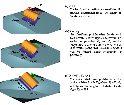
A sequence of pictures shows how the energy bands of HELLISH
are tilted by longitudinal electric fields.
High electric field carrier dynamics of HELLISH devices have
also been developed. Briefly, it involves electric field induction heating of
mobile carriers, i.e., hot electrons and holes, in their respective channels.
Hot electrons are injected into the quantum well via tunneling and thermionic
emission. The well acts as a giant trap for the hot electrons diffusing or
drifting into the depletion region.
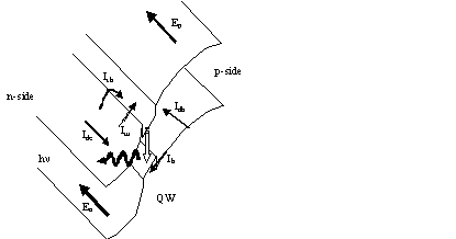
The HELLISH-1 energy band profile with the QW on the n-side
of the depletion region of AlxGa1-xAs p-n junction.
En,p are the electric fields applied parallel to the layers.
The injection of non-equilibrium carriers from the 3D AlxGa1-xAs
layer into the first sub-band of the GaAs QW is via Ith
(thermionic)
and Itu (tunnelling) currents. Ideand
Idh are the electron and hole drift currents in the
QW, respectively. Ihis the hot hole injection into
the well.
LOW FIELD OPERATION: QUASI FLAT-BAND CONDITION
One of the most important features of HELLISH device is the
bidirectionality in terms of the polarity of the applied voltage. The emission
region can be changed if the polarity of the applied voltage is reversed.
Therefore, it displays optical XOR logic functions by its bidirectional
property.
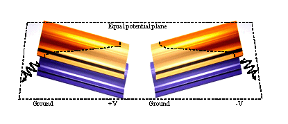
Illustration of bidirectionality of HELLISH devices with
different biasing polarities. Left: the device is positively biased and light
emission is from the left. Right: the device is negatively biased and light
emission is from the right.
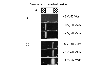
Infrared photographs, illustrating the growing emission
region of a 1 mm UB-HELLISH device (the schematic is shown on top of the photos)
with increasing fields. G = Ground. (a) positive polarity and (b) negative
polarity.
VCSEL-HELLISH
The VCSEL consists of a HELLISH-1 cavity surrounded by upper
and lower DBRs. The lower DBR provides a reflectivity in excess of 99%, while
the reflectivity of the upper DBR is slightly lower to allow an output from the
top surface. The QW is centralized within the cavity so that it is aligned to
the anti-node of the confined optical field, and therefore, maximises gain with
each round trip. The reflectivity and EL spectra of VCSEL-HELLISH are shown in
figures below.
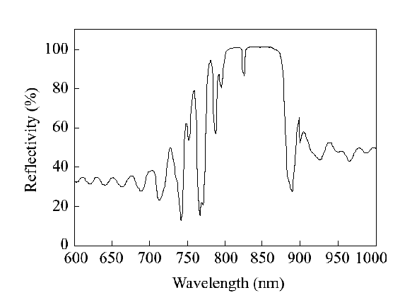
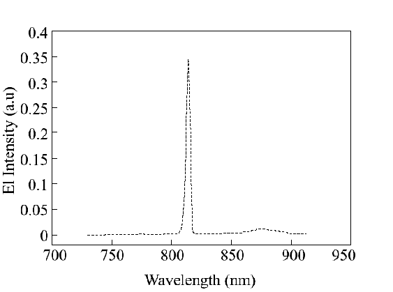
The reflectivityand EL spectrra of VCSEL-HELLISH.
TOP-HAT HELLISH (THH) WAVELENGTH CONVERTER
Unlike the standard HELLISH devices, the THH device is
fabricated to a shorter n-channel than p-channel by etching. Ohmic
contacts to the two channels are formed using Au-Zn and Au-Ni-Ge systems for the
p-type and n-type contacts, respectively. Under normal operation,
the device is biased with ±V at contacts 1 and 2, while contacts 3 and 4 are
grounded. When the device is biased with the positive polarity the potential
near to contact 2 (l2) is higher in the n-channel than
the p-channel (Vn>Vp). This results
in an effective reverse biased region, which acts as a light absorber. In
contrast, the area near to contact 3 (l3) is effectively
forward biased by the field, and therefore, can act as an emission region. In
other words, owing to the shorter n-channel length, the applied electric field
in the n-channel is higher than that in the p-channel, since both
channels are equally biased. Because of the different electric field strengths
within these channels, the energy band profile of the device is altered. The
built-in potential barrier of the p-n junction is enhanced near the anode
(drain) and flattened near the cathode (source). The reverse and forward biased
regions of the THS can be interchanged simply by changing the applied field
polarity It can, therefore, operate as a bi-directional field effect light
emitter/detector. Another potential application would be the self-pulsation
device, since it consists of both emission and absorption regions. The THH has
been demonstrated as an all-optical wavelength converter (down conversion),
using the set-up below
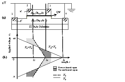
(a) Schematic of the THS device; (b) Illustration of the
potential distributions along the n- (broken line) and p- (solid
line) channels of the device. In the region Vn>Vp,
the device is effectively reverse biased; and in the region Vp>Vn,
it is effectively forward biased.
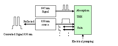
Illustration of THH as a multiple-wavelength converter.
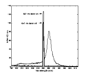
Reflected spectra of the THH operating as a wavelength
converter. The 850 nm light is modulated with the 647 nm incoming signal.
Applied voltage Va = 6.5 V, 647 nm laser power =70 mW.
VCSOA HELLISH
Semiconductor optical amplifiers (SOAs) have become an
important component of optical fiber networks in recent years. Many of the early
SOA devices were based on Fabry Perot cavity lasers, since then a number of
advanced structures, such as the traveling-wave amplifier (TWA), have been
demonstrated leading to improved performance. Similarly, vertical cavity SOAs
(VCSOAs),
which have attracted considerable interest in recent years, have been
demonstrated, and offer a number of potential advantages over conventional
in-plane edge-emitting SOA devices. Main advantages are lower cost, inherent
polarization insensitivity, higher fiber coupling efficiency, lower noise figure
and potential for integration into high-density two-dimensional array
architectures. So far, only a limited number of VCSOAs have been reported in the
literature. These include both optically and electrically pumped devices
operating at 1550 nm as well as an optically pumped 1300 nm device. Each of
these devices has a structure similar to that of standard VCSELs. The bottom
mirrors of these devices are produced to have reflectivities close to unity;
this is achieved using many period of DBR stacks. In contrast, the top mirrors
have relatively a few DBR periods. The lower reflectivity of the top mirror can
provide enhanced absorption of pump power (optically) in quantum wells, as well
as maximizing the gain-bandwidth production of the VCSOA. The low reflectivity
of the top DBR designed for operation in reflection mode requires multiple
quantum wells in the active region to give high single pass gain.
We have previously demonstrated several novel longitudinal
transport surface-emitting HELLISH devices. In this work, we used THS for the
VCSOA wafer with a short n-channel and a longer p-channel. The THS allows
different fields to be applied across the n- and p-channels.
Because of these different electric field strengths in the channels, the energy
band profile of the THH device can be twisted resulting in an emission region
and an absorption region within the same junction plane. It has, therefore, the
essential elements required to construct a compact wavelength converter, which
has been demonstrated at wavelength of 850 nm and 1.3 m
m. The most interesting potential application of the THH-VCSOA is a single
device which acts as a combined wavelength converter and optical amplifier.